

Key facts
- Samsung Electronics said Chairman Lee Jae-yong met researchers at the Yokohama Advanced Package Lab on November 1, 2026.
- Samsung Electronics said it plans to invest 350 billion won (US$262 million) in the lab over five years through 2028.
- Samsung Electronics said it held an opening ceremony for the Yokohama facility in September 2026.
- Samsung Electronics said Lee discussed cooperation with Japanese materials, components and equipment companies.
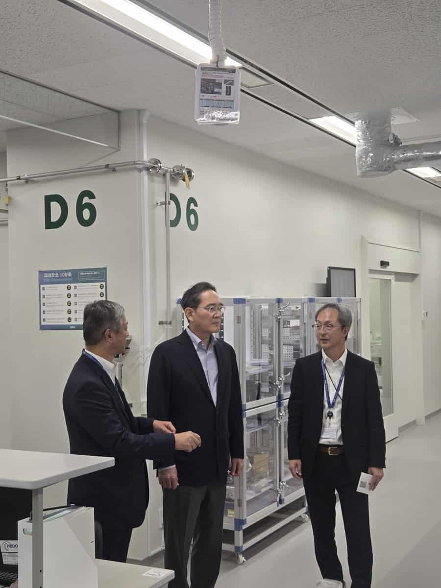
Samsung Electronics Co. Chairman Lee Jae-yong visited the company's Advanced Package Lab in Yokohama, Japan, Samsung said on Sunday, November 1, 2026. The lab is intended as a global research and development hub for technologies that improve the performance of artificial intelligence chips.
Samsung said it held an opening ceremony for the facility in September. The lab develops and validates materials and processes needed for advanced semiconductor packaging, drawing on Japan's materials, components and equipment industries, the company said in a press release.
During a meeting with researchers, Lee discussed progress on key packaging materials and process technologies and ways to deepen cooperation with Japanese companies in those supplier sectors, Samsung said. He stressed the importance of securing advanced packaging technologies, which the company described as essential to remaining competitive in the semiconductor industry in the age of AI.
Samsung established the lab in 2023 and spent the following two years preparing the facility and running initial research before the official opening in September, a company spokesperson said. Samsung plans to invest 350 billion won (US$262 million) in the research facility over five years through 2028.