Key facts
- IBM has developed a new 'nanostack' chip architecture.
- This technology is presented as the world's first sub-1 nanometer chip technology.
- The architecture vertically stacks transistors to enhance density and performance.
- IBM projects potential gains of 50% in computing performance or 70% in energy efficiency compared to its previous 2-nanometer node chips.
- The technology also shows a 40% improvement in scaling for static random-access memory (SRAM).
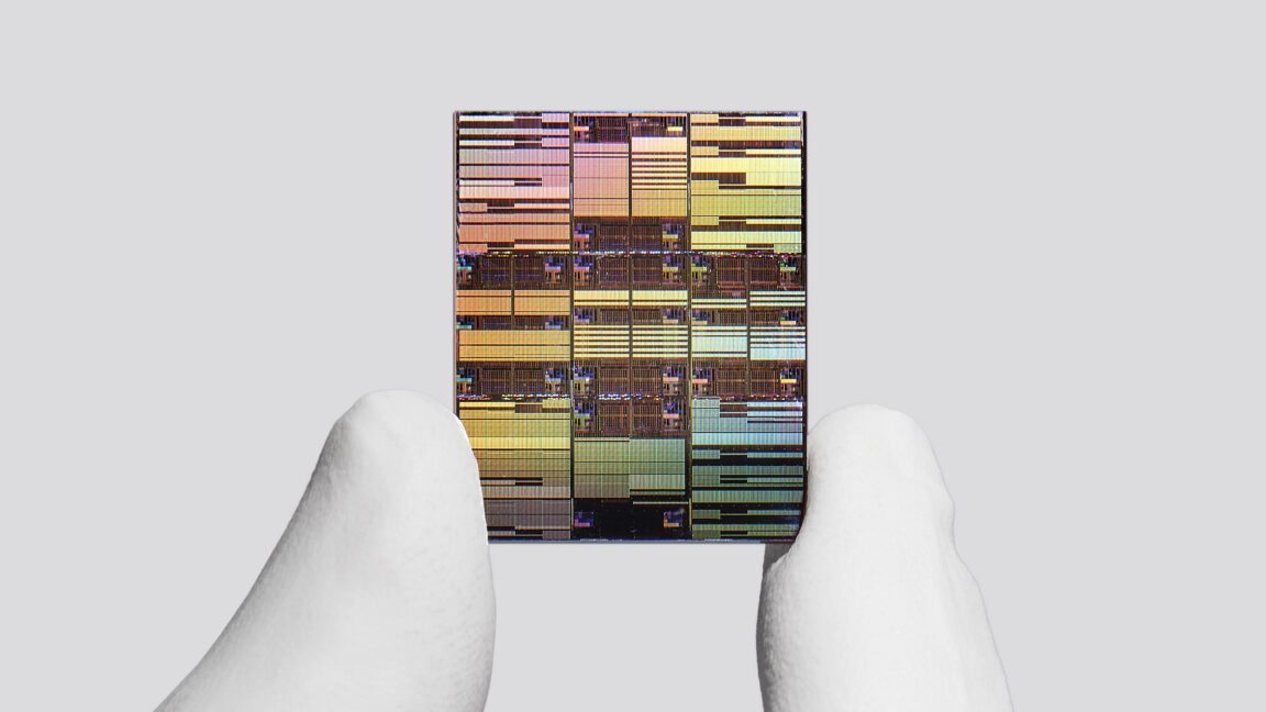
IBM has unveiled what it describes as the world's first sub-1 nanometer chip technology, named 'nanostack.' This new architecture allows for nearly 100 billion transistors to be integrated onto a chip the size of a fingernail, nearly doubling the transistor density of its previous generation. The company claims this advancement will lead to significant improvements in computing performance and energy efficiency, particularly for AI data centers.
The 'sub-1 nanometer' designation refers to the 0.7-nanometer node, which IBM calls the 7 angstrom node. However, IBM clarifies that these node numbers do not reflect the actual physical dimensions of the chip features, a trend that has been true for decades. Instead, the nanostack architecture achieves its density by vertically stacking transistors in a staggered layout, building upon IBM's prior nanosheet transistor development.
Each basic unit of the nanostack architecture consists of two stacked transistors, with each transistor containing three nanosheets. IBM projects that this technology could deliver 50% higher computing performance or 70% greater energy efficiency compared to its 2-nanometer node chips. The company also demonstrated a 40% improvement in scaling for static random-access memory (SRAM), a crucial component for AI workloads.
While IBM focuses on research and development, it partners with semiconductor manufacturers like Rapidus and Samsung to commercialize its chip technologies. IBM expects that chips incorporating the nanostack architecture could enter production within the next five to ten years, potentially becoming the mainstream technology for CPUs and GPUs, replacing current nanosheet technology.