Key facts
- Chinese chip design software firms are supporting Huawei's new "Tau Scaling Law".
- Empyrean Technology launched its Argus platform for 3D IC design, compatible with Huawei's methodology.
- Peking University developed a prototype EDA tool for Huawei's LogicFolding architecture.
- Huawei's "Tau Scaling Law" aims to improve chip performance by reducing signal travel time through vertical stacking.
- The approach seeks to circumvent US sanctions on advanced lithography equipment.
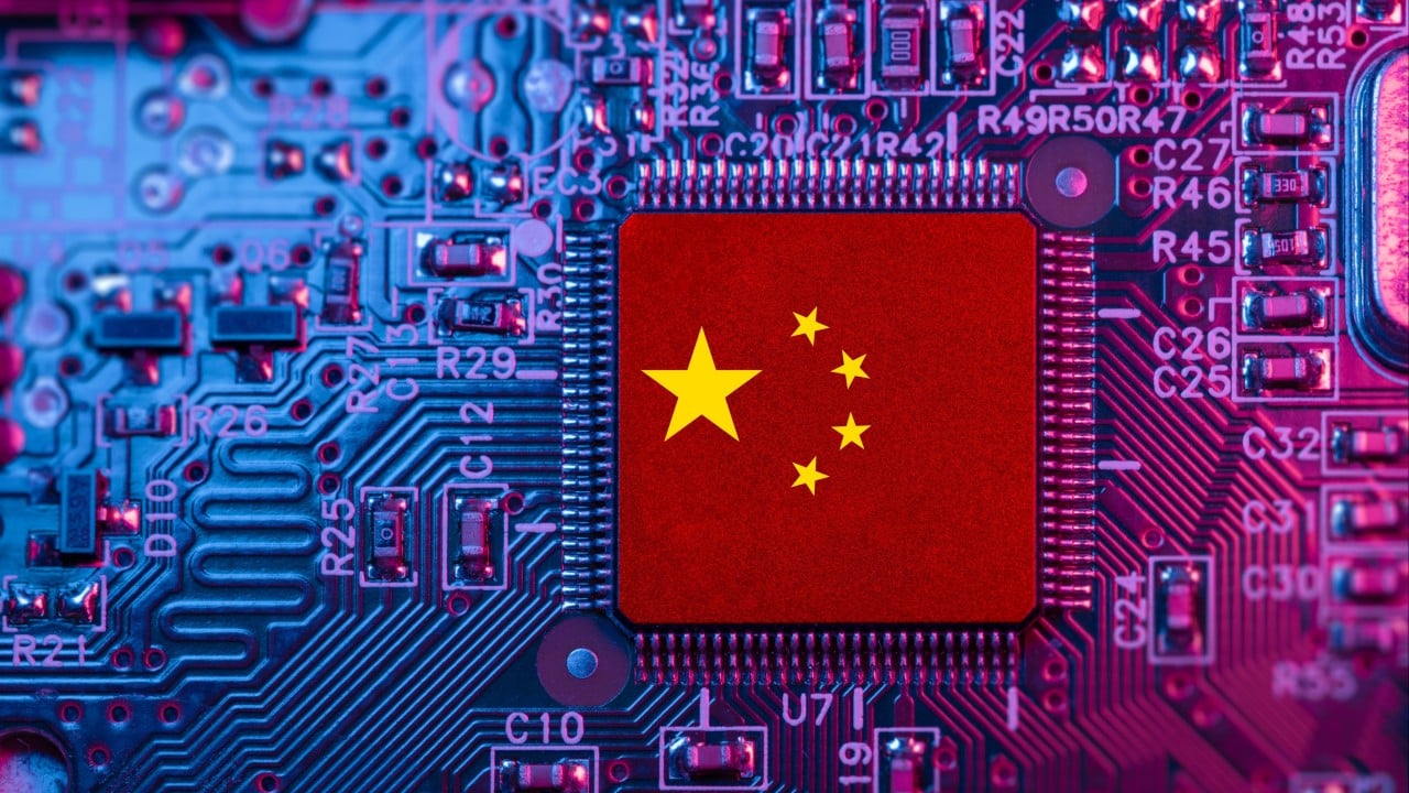
China's domestic chip design software industry is aligning behind Huawei Technologies' novel "Tau Scaling Law," a new chipmaking methodology designed to compete with leading global products. Empyrean Technology, a significant Chinese electronic design automation (EDA) provider, recently announced its Argus platform, a physical verification tool for three-dimensional integrated circuit (3D IC) design, which it has integrated into its expanding suite of tools. Empyrean described 3D IC technology as a crucial element for implementing Huawei's "Tau Scaling Law."
This development follows a claimed breakthrough by Peking University researchers, who introduced a prototype EDA tool utilizing a "true-3D" approach compatible with Huawei's "LogicFolding" architecture. This milestone occurred shortly after Huawei unveiled its "Tau Scaling Law" framework late last month. The "Tau Scaling Law" is presented as an alternative to Moore's Law, shifting the focus of chip development from shrinking transistors to reducing signal travel time across a system. By stacking flat circuits vertically into 3D structures through "LogicFolding," the approach aims to achieve transistor density and performance comparable to leading-edge chips without relying on advanced Western lithography equipment, which is subject to US sanctions. Despite this unified push, analysts caution that Chinese players face a considerable challenge in overcoming the established market dominance of US rivals.