All NewsEducationTVBrokers
Equities & FundsCrypto & Digital AssetsAI & TechnologyBusiness & CorporateUS Politics & PolicyGeopolitics & Global RiskMacro, Rates & FXCommodities & EnergyEuropean Politics & MarketsAsia-PacificReal Estate & Property
All NewsHome
← Back to AI & Technology

Samsung opens Japan AI chip R&D hub for advanced packaging collaboration

Created at 8 Sep · 4:16 PM1 source↑ Market-relevant
IN SHORT

Samsung Electronics has opened an advanced semiconductor packaging research and development center in Yokohama, Japan. The facility aims to foster collaboration with Japanese suppliers to enhance AI chip performance through innovative back-end manufacturing processes.

Key Numbers

¥25 billioninitial investment
$170 millioninitial investment
¥40 billionplanned investment over five years
100 employeestarget research team size by 2027
March 2027expected operational date for pilot production

Who's Involved

Samsung Electronics
Opened advanced AI semiconductor research center in Yokohama, Japan
Resonac
Japanese supplier collaborating with Samsung
Namics
Japanese supplier collaborating with Samsung
Disco
Japanese supplier collaborating with Samsung
University of Tokyo
Source of elite talent for Samsung's research center
Samsung opens Japan AI chip R&D hub for advanced packaging collaboration

↳ Why This Matters

This initiative highlights the intensifying global competition in AI semiconductor technology and the strategic importance of advanced packaging. By forming cross-border alliances, Samsung aims to accelerate innovation and close the gap with competitors like TSMC, underscoring the critical role of specialized materials and equipment suppliers in the future of high-performance computing.

Key facts

  • Samsung Electronics has opened an advanced semiconductor packaging research and development center in Yokohama, Japan.
  • The facility aims to foster collaboration with Japanese companies specializing in back-end chipmaking processes.
  • The center will focus on enhancing AI chip performance through innovative packaging technologies.
  • Samsung plans to invest approximately ¥40 billion over five years to expand the lab's infrastructure and research team.
  • The lab is expected to be fully operational with pilot production lines by March 2027.

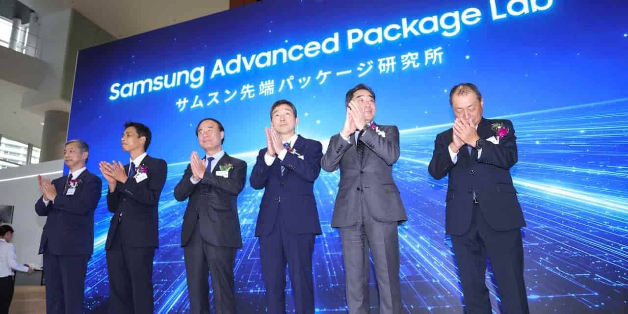
Samsung Electronics has inaugurated an advanced semiconductor packaging research and development center in Yokohama, Japan, on September 8, 2026. The facility, representing an investment of approximately 25 billion yen ($170 million), is designed to bolster Samsung's 2.5D and 3D chip packaging capabilities by leveraging Japan's expertise in semiconductor materials and dicing equipment. This strategic move aims to enhance AI chip performance through closer collaboration with Japanese industry leaders such as Resonac, Namics, and Disco, and to recruit top talent from institutions like the University of Tokyo.

The establishment of the Advanced Package Lab (APL) signifies a broader trend in the AI semiconductor landscape, shifting from individual corporate competition to cross-border alliances. Samsung plans to invest an additional ¥40 billion over five years, starting in 2024, to expand the APL's research infrastructure and grow its research team to over 100 employees by 2027. The lab is anticipated to be fully operational with pilot production lines by March 2027. This initiative is crucial as advanced packaging becomes increasingly vital for AI and high-performance computing devices, offering greater bandwidth and performance by integrating multiple components like GPUs and high-bandwidth memory (HBM) within a single package.

Frequently asked questions

The center aims to speed up technological advances in AI chip packaging by fostering close collaboration between Samsung and Japanese companies that are leaders in back-end chipmaking processes.

Samsung has invested approximately 25 billion yen ($170 million) initially and plans to invest an additional ¥40 billion over five years, starting in 2024.

Samsung is collaborating with industry leaders such as Resonac, Namics, and Disco.

The lab is expected to be fully operational with pilot production lines by March 2027.

What Happens Next

01The lab is expected to be fully operational with pilot production lines by March 2027.
CME Headlines
  • Risk Management and Monitoring Notice: Multi-Factor Authentication Updates - September 12
    3 Sep · 5:00 AM

How It Developed

Samsung Electronics opened an AI chip packaging research center in Yokohama, Japan.
The facility represents an investment of approximately 25 billion yen ($170 million).
Samsung plans to invest approximately ¥40 billion over five years, beginning in 2024.
The company plans to increase the research team to more than 100 employees by 2027.
The lab is expected to be fully operational with pilot production lines by March 2027.

Sources

T1
Samsung opens Japan AI chip R&D hub for advanced packaging collaborationNikkei Asia
T2
Samsung Electronics opens packaging lab - Advanced Packaging Newsadvancedpackaging.news
T2
Samsung Electronics opens AI semiconductor research center in Yokohama ...thebuildout.ai

Related Stories

ASML to Supply Advanced EUV Tools to TSMC, Samsung, Intel by 2030
8 Sep · 9:36 AM
Philippines unveils $34.4bn AI infrastructure plan to become regional hub
8 Sep · 8:46 AM
Qualcomm, Amazon Forge Multi-Generational AI Chip Pact
8 Sep · 1:19 PM
AI, chip firms among bidders for Hong Kong tech hub
8 Sep · 12:35 AM
Goldman Sachs opens AI engineering hub in Bellevue
8 Sep · 3:06 PM