Key facts
- ASML is developing hybrid bonding equipment, a technique for directly joining chips or wafers.
- The company filed 27 patent families related to hybrid bonding tools between December 2022 and November 2024.
- ASML is collaborating with Prodrive Technologies and VDL ETG on the development.
- Hybrid bonding enables higher interconnect density and lower resistance compared to traditional methods.
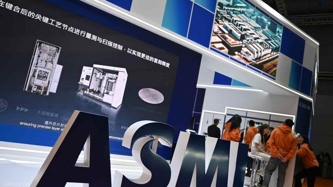
ASML is reportedly developing equipment for hybrid bonding, a next-generation chip packaging technique that creates dense electrical connections by directly joining chips or silicon wafers. The Dutch semiconductor equipment maker submitted 27 patent families related to hybrid bonding tools between December 2022 and November 2024, according to a report by semiconductor and AI supply chain research firm SemiAnalysis. The company is collaborating with long-standing suppliers Prodrive Technologies and VDL-ETG on the development of these systems.
Hybrid bonding directly connects copper surfaces between chips, enabling higher interconnect density and lower resistance compared to traditional methods like thermocompression bonding. This technology is seen as critical for improving chip performance and is being adopted by major Chinese companies. ASML's move into this market is not unexpected, as the company has previously introduced back-end systems for advanced packaging and its CTO has indicated an evaluation of opportunities in this sector.
Other industry players are also active in the hybrid bonding space. Equipment supplier Besi reported a significant increase in its backlog driven by hybrid bonding demand, and ASMPT also sees advanced packaging as a key revenue contributor. Applied Materials has partnered with Besi to develop a hybrid bonding system.