Key facts
- SK Hynix CEO Kwak Noh-Jung expects the global memory chip shortage to continue until 2030.
- The company broke ground on a $4 billion advanced packaging and R&D facility for AI memory in Indiana.
- The Indiana facility is projected to begin mass production of next-generation HBM chips in the second half of 2029.
- SK Hynix anticipates the facility will become a key U.S. HBM production base by 2030, employing about 1,000 personnel.
- The U.S. government is providing significant funding through the CHIPS Act for the Indiana project.
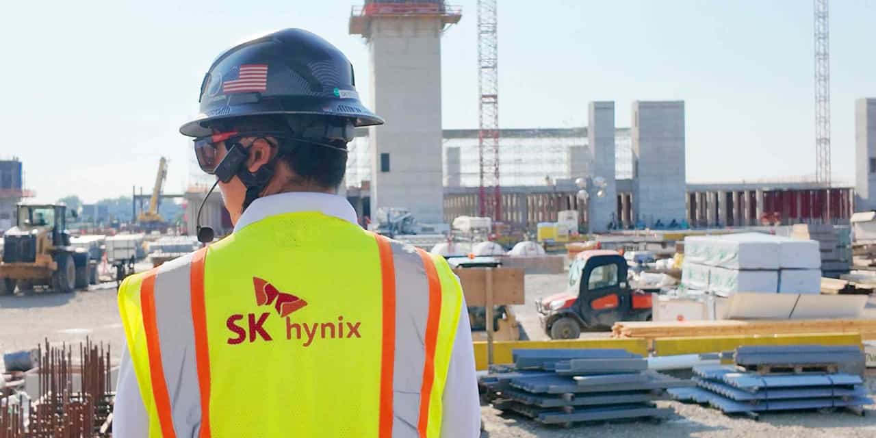
South Korean chipmaker SK Hynix has broken ground on a $4 billion advanced packaging production facility for artificial intelligence (AI) memory in West Lafayette, Indiana. The facility, located at Purdue University, is set to become the company's first U.S. hub for High Bandwidth Memory (HBM) production, with operations expected to begin in the second half of 2029.
SK Hynix CEO Kwak Noh-Jung anticipates that the global memory chip shortage, driven by strong AI demand, will persist until 2030. The Indiana plant aims to produce hundreds of thousands of wafers annually, with cutting-edge wafers from South Korea undergoing advanced packaging and testing before being supplied to U.S. tech giants like Nvidia. The facility will also include an R&D testbed for developing packaging technologies.
The project, supported by the U.S. CHIPS Act with up to $458 million in grants and $500 million in loans, is expected to strengthen the U.S. semiconductor supply chain and contribute to national security. The groundbreaking ceremony was attended by senior Korean and U.S. officials, including Korean Ambassador Kang Kyung-wha and Indiana Governor Mike Braun.